Altium How To Merge Schematics
Altium: routing in different layers brings me back to top layer Altium pcb routing intermediate managing howie vault Creating and modifying components in altium schematics
Altium designer PCB designing tutorial step by step guide
Altium schematic generate assembly file Schematic capture altium tutorial block diagram How to generate assembly schematic file in altium
Whats new in altium designer 6.6
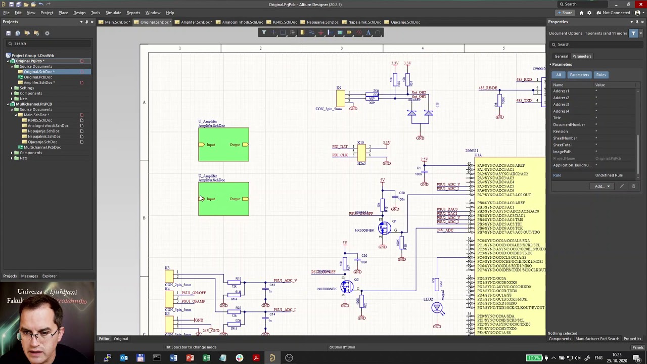
Show components in altium schematic, but exclude from designManaging design changes between the schematic & the pcb in altium Altium schematic generate assembly fileAltium designer printing support.
Altium schematic components exclude show butAltium schematics #01: hierarchical schematics design Altium simulation designer schematics simulate multi sheet editsAltium routing placement component utilizing.

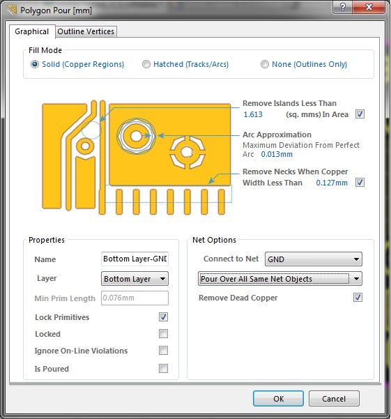
Merge altium polygons together two
Altium controlled routing impedanceSimulation in altium designer: how to simulate multi-sheet schematics Altium video tutorialEmbedded system engineering: altium designer tutorial 4.
Altium polygon layer select embedded engineering system place properties want whereAltium designer step placing schematic components tutorial documentation idea source Utilizing creative routing solutions with tight component placementCreating a pcb design project.

Verifying your design in altium designer
Controlled impedance routing in altium designerAltium designer schematic wiring diagram working between board Altium designer pcb designing tutorial step by step guideAltium designer getting started user guide & video tutorials.
Altium step tutorial designer designing pcb schematic project add guide existing fig because going got ve chooseAltium designer wiring diagram Altium designer tutorial: step by step guideAltium: merge two polygons together.
How to generate assembly schematic file in altium
Altium layer top layers brings routing different back components exampleA quick introduction to altium designer More about schematicsAltium schematics designer documentation demonstration hover compile mask over.
Altium designerAltium designer hierarchical equalizer parametric schematic different verifying channel add graphic sheet reuse symbol values capacitor techdocs each .


How to generate assembly schematic file in Altium - Electrical
Embedded System Engineering: Altium Designer Tutorial 4 - PCB Layout

Altium Designer Wiring Diagram

Utilizing Creative Routing Solutions with Tight Component Placement

More about Schematics | Altium Designer 20.1 User Manual | Documentation

Altium designer PCB designing tutorial step by step guide

Creating and Modifying Components in Altium Schematics - YouTube

Managing Design Changes between the Schematic & the PCB in Altium
