Cmos Nor Gate Stick Diagram
Cmos gate nand nor structure Gate nand stick diagram layout cmos aoi flip flop adder triggered edge invert example draw vp latch implemented transcribed text Gate cmos nor circuitry instrumentationtools
NOR Gate(2 input) layout | All For Students
Nand cmos vlsi layout nor daigram jce transistor diffusion layouts Solved: chapter 1 problem 11e solution Cmos nor vlsi 11e
1 (a) structure of a cmos gate. (b) cmos-nand. (c) cmos-nor.
Solved draw the stick diagram for a 2-1 aoi (and-or-invert)M02 lec09 cmos 3 input nor gate stick diagram Cmos gate circuitry instrumentation toolsExperiment 2 layout of 2 input cmos nor gate using microwind.
Nand stick diagramSolved: chapter 1 problem 10e solution Input gate cmos nor diagram stick schematic transistor sketchLayout nor input gate.

Nor gate diagram cmos stick input
Diagram stick nand gate input cmos driving problem twoNor gate(2 input) layout Nor cmos inputNand stick diagram.
.


Nand Stick Diagram - Wiring Diagram Pictures

M02 Lec09 CMOS 3 Input NOR Gate Stick Diagram - YouTube

Nand Stick Diagram

CMOS Gate Circuitry Instrumentation Tools

Solved: Chapter 1 Problem 10E Solution | Cmos Vlsi Design 4th Edition

1 (a) Structure of a CMOS gate. (b) CMOS-NAND. (c) CMOS-NOR. | Download

Solved: Chapter 1 Problem 11E Solution | Cmos Vlsi Design 4th Edition
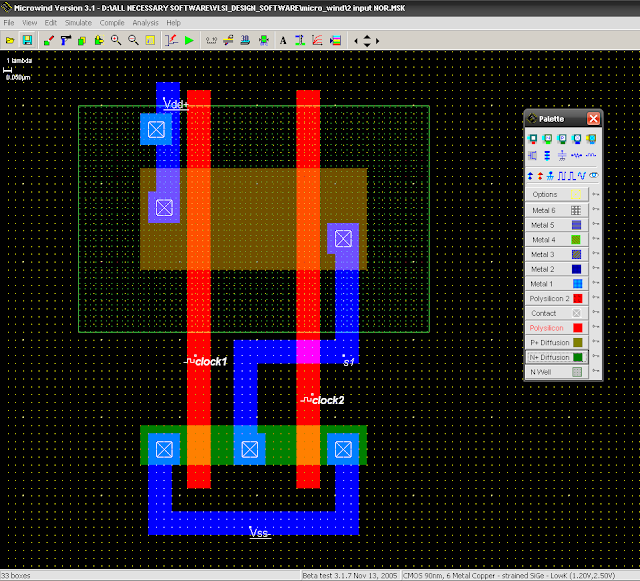
NOR Gate(2 input) layout | All For Students
